


Showing result 1 to five of 30 essays containing the text PHASE LOCKED LOOP.
1. System Level Modeling and Verification of-digital Phase-locked Loop
College essay from KTH/Skolan fr informations- och kommunikationsteknik (ICT)
Abstract. In wirelesscommunication systems, a detailed oscillator (LO) targets demodulating radio-frequency signals into baseband signals. The performance of people signals determines the standard of communications that’s highly affected by the phase precision of local oscillators. Find Out More
2. Analysis and improvement of phase noise performance in the PLL-based RF synthesizer
College essay from Chalmers tekniska hgskola/Institutionen fr mikroteknologi och nanovetenskap
Abstract. The objective of this thesis work ended up being evaluate, model and raise the phase noise performanceof a wideband synthesizer prototype. The examined synthesizer draws on aphase-locked loop (PLL) through getting a dynamic loop filter, in which the output frequency range is2340MHz 4420MHz in steps of 260MHz. Find Out More
3. Timing and Synchronization over Ethernet
College essay from Linkpings universitet/Institutionen fr systemteknikLinkpings universitet/Tekniska hgskolan
Abstract. During this thesis an analysis will probably be performed about how precisely serious amounts of frequency may be synchronized over Ethernet with help of Precision Time Protocol and Synchronous Ethernet. The aim should be to obtain a high precision within the synchronization every time a topology of 10 cascaded nodes can be utilized. Find Out More

4. Firmware Design and Implementation for almost any 14-bit Analog-to-Digital Ripping tools for use within the PANDA Experiment
College essay from Uppsala universitet/Institutionen fr informationsteknologi

Abstract. Advancement of the VHDL firmware for almost any high-speed Analogue to Digital Ripping tools (ADC) may be the focus in the paper, including writing, debug- ging and look for pointed out firmware. The finished kind of the firmware is able to properly convert analogue signals received using the ADC for his or her digital representations. Find Out More
5. Construction in the low-ripple inverter with accurate phase control for calibration of measurement equipment
College essay from Chalmers tekniska hgskola/Institutionen fr energi och milj
Abstract. For the perception of an electrical power system, understanding within the parameters of all of the componentsis essential. Specifically the transformers are a fundamental element of the. It’s thereforeimportant the measurement equipment for exercising these values is accurate. Inno-load operation, the transformer mainly consumes reactive power. Find Out More
Our Guarantees Our Quality Standards Our Fair Use Policy
How Come United kingdom Essays Different?
- There is a verifiable exchanging history as being a United kingdom registered company (details within the finish of every page).
- Our Nottingham offices are suitable for purchase to everybody to satisfy we greater than 40 full-time staff.
- United kingdom Essays partner with Feefo.com to produce verified customer testimonials – both positive and negative!
Ask an expert FREE
Ask an expert Index Ask an issue Compensated Services

About Our Ask an expert Service
Our free of charge “Ask a specialistInch Service enables users to get a solution as much as 300 words for the academic question.
- Questions typically clarified within 24 hrs.
- All solutions are researched and printed by properly accredited academics within the question’s market.
- Our services are totally private, only the solution is printed – we never publish your very own details.
- Each professional answer includes appropriate references.
About Us
More Details On Us
Keywords: Digital PLL, Digital Phase/Frequency detector, NCO (time for you to digital ripping tools plus digitally controlled oscillator), Divide by N counter.
Introduction
PHASE LOCKED loops are broadly present in frequency synthesis applications [2], [4], [5]-[7]. For many portable applications the purchase length of PLL is essential so the perception of PLLs with minimum acquisition time may be the primary reason for the task .A Phase Locked Loop (PLL) could be a feedback system that blogs in regards to the output phase while using the input phase to create an output signal which has exactly the same phase as individuals from the port signal. PLL’s are available in lots of applications for example reference generation, frequency synthesis, frequency multiplication, FM demodulation. etc. Because the frequency of operation increases, involve generating signals which are in phase lock with input (i.e. fast different signals) has become an issue. There’s 2 types of PLL’s 1) Analog PLL 2) Digital PLL .Traditional PLL’s are analog PLL’s as proven in fig.1
Fig.1 Block diagram of Analog PLL
It uses phase detector to look for the input phase while using the output phase. Loop filter enables you to reduce the ripples across the control current of VCO. VCO enables you to regulate the output frequency therefore the loop is locked along with the output signal may be the replica within the input signal. However, analog PLL’s are bulky and fewer protected against noise. Whereas D-PLL’s are compact and guarded from noise. Additionally D-PLL’s are often programmable (i.e. easy process conversion).
D-PLL Architecture
The block diagram representation in the D-PLL is proven in fig.2. The below architecture is simple and quick to make use of.
Fig.2 Block diagram of D-PLL
The D-PLL architecture proven above has four major blocks, namely the phase/frequency detector (PFD), time to digital ripping tools (TDC), the accumulator along with the number control oscillator (NCO). The NCO is implemented by using frequency divider circuit. The PFD detects the phase or frequency one of the reference clock and output clock. The introduction of the PFD is supplied to TDC that’s continuous as time passes. Time to digital ripping tools generates a count value that’s proportional for that phase error. The standard value (Electricity value) within the PFD is accrued using the accumulator block. The accrued value determines the control word for the NCO to oscillate through getting a appropriate frequency.
Analysis of human Blocks
Phase Detector:
The Phase detector (PD) could be a circuit that blogs in regards to the phase difference backward and forward input signals. It makes an output signal whose average value is linearly proportional for that phase difference backward and forward input signals. You will find number of options where a Phase Detector may be recognized, but we mostly consider two kinds. They’re 1) XOR-gate 2) PFD.
XOR-Gate Phase Detector:
The XOR-gate (from Fig.3) produces an output when both input’s are unequal, otherwise zero.
Fig.3.1 Output waveform of XOR-Gate.
The XOR-gate produces output within the growing edge and falling side of the cycle. The below equation gives inside the input-output relationship in the XOR-gate Phase Detector.
Plagiarism-free
Always rapidly
Marked to plain
Fig.4 Input-Output characteristics of XOR-Gate Phase Detector
As you can noticed in the above mentioned pointed out characteristics, the issue of XOR-gate Phase Detector is its linearity range is bound to π. once the phase difference is a lot more than π then it’s average output value decreases. Therefore we choose switch-flop base phase Detector or Phase Frequency Detector.
Phase Frequency Detector(PFD):
Fig.6 Block diagram of PFD
Fig.7 Output waveforms of PFD
The circuit proven in fig.6 is both phase/frequency detector. It’s three states, initially both and other alike to zero. If input A leads input B, first goes filled with the growing side of input A (since relates to logic 1), then goes filled with the growing side of input B(since can also be connected with logic 1), inducing the introduction of the NAND gate to visit low. therefore resetting both and .Similarly if input B leads input A then goes high first.The circuit includes two positive edge triggered, negative edge resettable D-switch-flop getting tied their inputs to logical 1. The input’s appealing functions like a clock to alter-flop.The input output characteristics within the Phase Frequency Detector is proven below:
Fig.8 Input-Output characteristics of PFD
From fig.8, it’s apparent the primary benefit of Phase Frequency Detector is the fact it’s improved linearity range as well as the chance some factor just like a frequency detector too.
Integrator
The integrator block includes time for you to digital ripping tools plus discrete time accumulator (1 tap IIR filter).
Time For You To Digital Ripping tools:
Time to digital ripping tools block enables you to transform the introduction of the Phase Frequency Detector that’s continuous in a digital number. Time to digital conversion can be achieved simply employing a counter which is capable of doing counting up minimizing. The next analysis has proven the output count value is proportional for that input Phase Difference.
Fig.9. Time for you to Digital Ripping tools (TDC) implemented with Counters.
Fig.10. Output Waveforms of energy to Digital Ripping tools (TDC).
Let C= Counter Output
C (t) = time different condition of Up/Lower counter.
=Counter clock period.
T=duration of input or phase detector cycle period.
If is extremely small i.e. if then ∑ becomes integration.
If there’s N1 cycles in T seconds then
Where =counter clock frequency.
From equation (4) it’s apparent the output count value C is proportional for that input phase difference.
Accumulator (Discrete time integrator):
The accumulator block enables you to provide you with a constant number (control_word) for that Number Control Oscillator (NCO). The accumulator block can be compared for that LPF (integrator) in analog PLL.
Number Control Oscillator (NCO)
The Output frequency within the NCO is numerically controlled employing a binary word instead of current. This is actually the NCO generates an output signal whose frequency is proportional for that input control word (binary format). There are many strategies to implement NCO block but the easiest method to implement NCO is counter based approach. The NCO includes counter capable of dividing the input clock according to its control word. The applicability in the device as NCO is described below.
* Control word —— (1)
Where k= Resolution =. n= Amount of bits in counter.
The resolution of NCO increases by growing the amount of bits. The greater the control word, more regularity and vice-versa.
Fig.11 Block diagram of NCO
Fig.12 Internal block diagram of NCO
Fig.13 Input- output characteristics of NCO
From equation (1), it’s apparent the NCO may be implemented using counter, whose output frequency draws on the Control word. Probably the most input frequency which can be locked is dependent upon the NCO resolution (k=).The counter based NCO frequency range is
Experimental results
Fig.14 Output waveforms of PLL at 210MHz
Fig .14 shows the Output waveforms within the PLL in which the reference clock is 52.35MHz. The D-PLL is synthesized using pedal rotation RTL compiler in 45nm CMOS process. The D-PLL is implemented with following specifications:
This Essay is
This essay remains printed getting students. This isn’t one of the task printed by our professional essay authors.
Types of our work
Maximum NCO frequency = 209.42 MHz
Free running frequency of NCO = 130.8MHz.
NCO resolution = = 6.54MHz n=5 bit.
Input Frequency = 7MHz.
Table 1. Performance comparisons
Inside the above comparison table it’s apparent that power dissipation within the suggested D-PLL is minimal to another of Digital cell based PLL [1], Analog PLL [2], Semi-Digital PLL [3]. The purchase length of suggested D-PLL is under Digital cell based PLL[1] and analog PLL[2] i.e. suggested D-PLL is quicker in comparison with other two PLLs suggested in [1],[2].
Conclusion
Within the paper a D-PLL is presented. The D-PLL is implemented with standard cells within the .045µm technology and may operate from 6.54MHz to 105MHz. The presented D-PLL architecture is simple and quick to make use of.
Request Removal
If you’re the very first author in the essay with no longer want the essay printed across the United kingdom Essays website then please go here below to request removal:
More from United kingdom Essays
Fully referenced, delivered rapidly, Essay Writing Service.
Everything perform is focussed on writing the best assignment for your exact needs
Our Dissertation Writing service can deal with from full dissertations to individual chapters.
Our Free Marking Service can help you choose parts of the task that require improvement.
Try taking a little assist with an issue? We’ve over 500 academic experts waiting that will assist you, free of charge!
Everything you should know inside your studies
Tools that will assist you with the development of academic references in several styles.
Start the transaction now
Our experts will help you together with your essay

 Thesis writing schedule of craig
 Different research methods in thesis writing
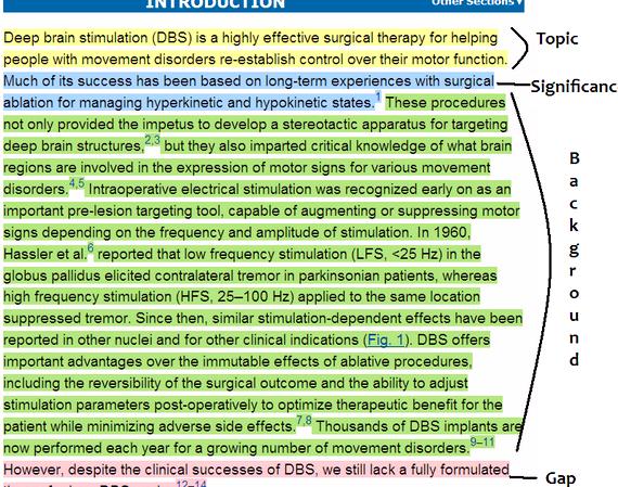 Writing a thesis introduction sample
 Lens induced glaucoma thesis writing
 John beatty evolutionary contingency thesis proposal


